Organic Field Effect Transistor
1. Dielectric surface Control
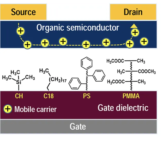
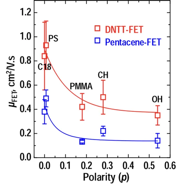
Physical or chemical properties characterizing a surface of gate dielectric have a huge impact on the electrical properties of organic field-effect transistors. Here, we applied various organic interlayers between an organic semiconductor and a gate dielectric to describe field-effect mobilities being a function of a certain macroscopic parameter associated with the surface energy of gate dielectric.
The organic interlayers with various chemical moieties, that is, hydroxyl, methyl, octadecyl, polystyrene, and polymethylmetacrylate, are obtained using diverse organosilane compounds and hydroxyl-end-terminated polymer brushes. Two prototypical vapor-deposited p-type organic small molecules, dinaphtho[2,3-b:2′,3′-f]thieno[3,2-b]thiophene and pentacene, are used as semiconducting layers.
We separate the surface energy of the organic interlayers into two terms, that is polar and dispersive terms, and define three parameters consisting of these two terms, so-called surface energy ratio, polar ratio, and polarity. The three parameters are plotted with the field-effect mobilities and it becomes apparent that the field-effect mobility is a function of polar ratio and polarity regardless of the semiconducting material as well as its morphology and crystallinity. In particular, the polarity that is the polar energy term divided by the total surface energy showed a clear exponential relationship, allowing a reliable prediction of field-effect mobilities.
OFET의 전기적 성능을 향상시키기 위한 주요 접근 방식 중 하나는 서로 다른 구성 요소의 계면, 특히 게이트 유전체와 유기 반도체 사이의 계면의 특성을 조절 하는 것이다. 유전체 표면이 유기 반도체 증착 동안 분자 조립을 담당할 뿐만 아니라 계면에서의 효율적인 전하 수송을 담당하기 때문에 이 계면은 OFET의 전하 수송 및 전기적 특성을 결정하는데 중요한 역할을 한다. 일반적으로 유기 반도체와 게이트 유전체 사이의 표면 에너지는 불일치하므로 유전체 표면의 물리적 또는 화학적 특성을 조절하여 이러한 표면 에너지의 불일치를 조정하기 위한 노력을 해왔다.
본 연구진은 게이트 유전체의 표면 에너지와 관련된 특정 거시적 매개변수의 함수인 전계 효과 이동도를 설명하기 위해 유기 반도체와 게이트 유전체 사이에 다양한 유기 중간층을 적용하였다. 히드록실, 메틸, 옥타데실, 폴리스티렌 및 폴리메틸메타크릴레이트를 갖는 다양한 유기실란 화합물 및 히드록실 말단 중합체 브러시를 사용하여 유기 중간층을 도입하여 다양한 화학적 특성을 제공하였다. 두개의 프로토타입 증착 p형 유기 소분자인 DNTT와 Pentacene이 반도체 층으로 사용되었으며, 유기 중간층의 SE를 극성 및 분산 term이라는 두가지 term으로 분리하고 OFET 장치에서 전하 이동성과 강한 관계를 같는 SE 관련 위한 세 가지 매개변수인 표면에너지 비율, 극성 비율 및 극성을 정의하였다. 결과적으로 반도체 물질에 관계없이 극성비와 극성의 함수인 전계 효과 이동도를 확인할 수 있었으며, 게이트 유전체의 표면 특성을 기반으로 OFET 성능을 예측하기 위한 간단한 기준을 제공할 수 있었다.
2. Organic Semiconductor Structural Control
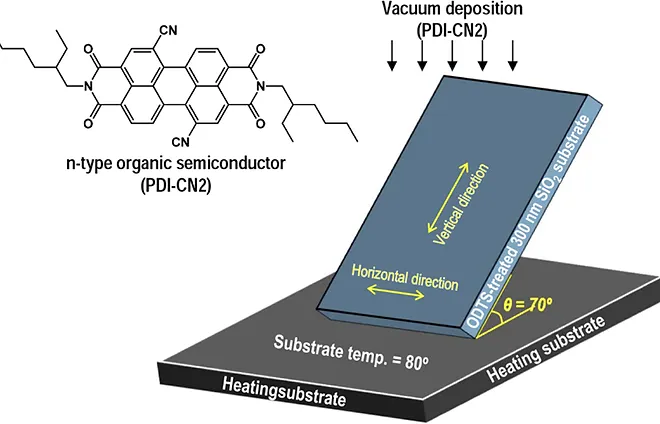
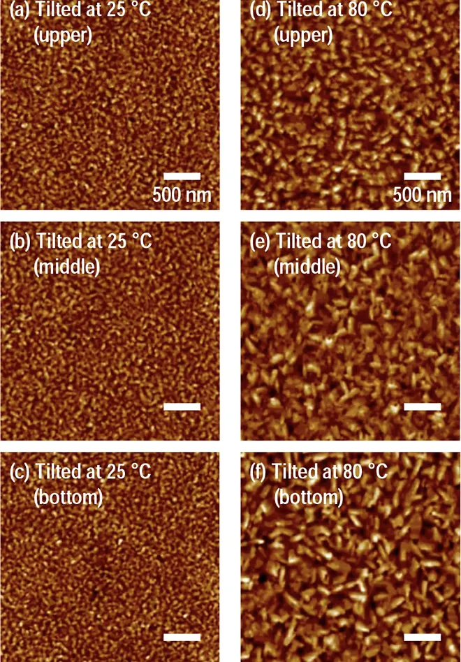
A thermal gradient distribution was applied to a substrate during the growth of a vacuum-deposited n-type organic semiconductor (OSC) film prepared from N,N′-bis(2-ethylhexyl)-1,7-dicyanoperylene-3,4:9,10-bis(dicarboxyimide) (PDI-CN2), and the electrical performances of the films deployed in organic field-effect transistors (OFETs) were characterized. The temperature gradient at the surface was controlled by tilting the substrate, which varied the temperature one-dimensionally between the heated bottom substrate and the cooled upper substrate.
The vacuum-deposited OSC molecules diffused and rearranged on the surface according to the substrate temperature gradient, producing directional crystalline and grain structures in the PDI-CN2 film. The morphological and crystalline structures of the PDI-CN2 thin films grown under a vertical temperature gradient were dramatically enhanced, comparing with the structures obtained from either uniformly heated films or films prepared under a horizontally applied temperature gradient.
The field effect mobilities of the PDI-CN2-FETs prepared using the vertically applied temperature gradient were as high as 0.59 cm2 V–1 s–1, more than a factor of 2 higher than the mobility of 0.25 cm2 V–1 s–1 submitted to conventional thermal annealing and the mobility of 0.29 cm2 V–1 s–1from the horizontally applied temperature gradient.
OSC 박막의 형태 및 결정 구조는 열 또는 용매 어닐링 및 용매 soaking을 포함한 다양한 공정 방법을 사용하여 OSC 분자의 자기 조직화 특성을 조절함으로써 개선될 수 있다. 열처리는 공정 온도와 시간을 조정하여 OSC 필름의 전기적 특성을 효율적으로 향상시키기 때문에 진공증착이나 용액 공정에 의해 OSC 분자 재배열 및 결정화를 제어하는데 널리 사용된다. 그러나 OFET의 성능은 열 에너지가 기판 전체에 무작위로 적용되기 때문에 단순히 열 어닐링 과정을 사용하여 개선하기 어렵다. 고성능 OFET 장치는 OSC 필름의 방향성 선택 성장을 통해 잘 제어된 필름 형태와 조직화된 결정 구조를 결합하여 얻을 수 있다. 특정 구역의 어닐링 방법은 국부적인 용융 및 냉각을 통해 방향성 재결정화를 달성하는 대표적인 방법으로, 여러 연구 그룹은 OFET에 구역 어닐링 과정을 적용하여 고성능 OFET 장치를 달성하였다. 그러나 구역 어닐링 과정은 최적의 방향, 속도 및 지연 시간을 보장하기 위해 조건을 세심하게 제어해야하므로 비효율적이다. 뿐만 아니라 펜타센과 같은 진공 증착된 소분자 OSC에 대한 구역 어닐링의 효과는 탁월하지 않았으며, 구역 어닐링은 용융 온도에 근접하는 매우 높은 온도를 요구한다.
본 연구진은 기판에 열 구배를 적용하여 열증착 OSC의 박막 성장을 조절하기 위한 효율적인 전략을 시연하였다. 온도 구배는 가열판에서 기판을 수직으로 기울여서 바닥과 위쪽에 각각 높은 기판 온도와 낮은 기판 온도를 유도하여 형성시켰다. 기울어진 기판은 OSC 분자의 증착 동안 사용되어 수직 방향을 따라 더 높은 결정도와 우수한 전기적 특성을 가진 필름을 생성하였다. n형 OSC 물질인 PDI-CN2를 사용하여 이 온도 구배 방식을 적용하여 FET의 전계 효과 이동도는 0.59cm2 V-1 s-1를 기록하였다. 이는 0.25cm2 V-1 s-1의 기존 열 어닐링을 사용하여 제작된 OFET 장치에서 얻은 값을 훨씬 초과하는 값을 달성하였다(그림 3c).
Printed Electronics
1. Spray Coating
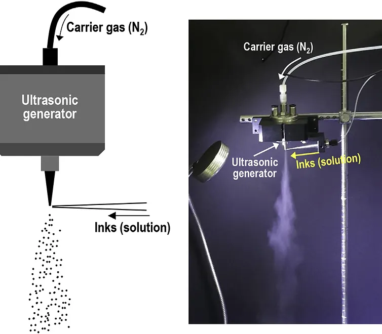
The ultrasonic nozzle (US) spray method was investigated for its utility in fabricating organic electrodes composed of poly(3,4-ethylenedioxythiophene):poly(styrenesulfonate) (PEDOT:PSS), a standard conductive polymer material used to produce large-area low-cost OFETs. The US spray technique involves generating a solution spray by first passing the solution through a head and nozzle subjected to ultrasonic vibrations that induce atomization. This method is advantageous in that the resulting spray comprises extremely small solution droplets a few micrometers in diameter, unlike the spray produced using conventional air spray methods. The PEDOT:PSS US solution spraying process was optimized by controlling the flow rate of the N2 carrier gas and the substrate temperature while monitoring the quality of the resulting PEDOT:PSS electrode films. The pentacenefield-effect transistors prepared using the US spray method displayed a maximum field-effect mobility of 0.47 cm2V−1s−1 (with an average value of 0.31 cm2V−1s−1), 35% better than the mobilities achieved using the conventional air spray method. In addition, the device-to-device reproducibility was improved, as indicated by a decrease in the standard deviation of the mobility values from 30% for the air spray devices to 24% for the US spray devices. These results indicated that the US spray technique is efficient and superior to the conventional air spray method for the development of low-cost large-area organic electronics.
에어 스프레이 프린팅 방법은 넓은 면적에서 균일한 코팅 품질을 제공할 수 있어 저가의 유기 박막을 제조하기 위해 일반적으로 사용되는 용액 공정 기술이다. 하지만 에어 스프레이 프린팅 기술은 노즐에서 토출되는 용액 방울의 직경이 50~1000um 범위이기 때문에 고정밀도와 균일한 표면 코팅을 달성하는데 어려움이 있다. 따라서 최근에는 이러한 에어 스프레이 프린팅 방식을 보완하기 위해 초음파 노즐 스프레이 방식이 도입되었다. 초음파 노즐 스프레이 기술은 용액이 분사되는 노즐에 초음파 진동을 가하도록 설계된 코팅 장비이며, 용액은 2~5um의 매우 작은 액적으로 토출되므로 기존의 스프레이 코팅 방법에 비해 미세하고 균일한 유기 필름을 제작할 수 있다.
본 연구진은 저비용 대면적 OFET 제작에 일반적으로 사용되는 전도성 고분자 재료인 PEDOT:PSS로 초음파 노즐 스프레이 방식을 이용한 유기 전극을 제작하였다. 최적의 초음파 노즐 스프레이 조건을 조사하기 위해 N2 가스의 유량과 기판 온도를 조절하였으며, OFET 소자의 활성층은 표준 유기 반도체 재료인 펜타센을 사용하였다. PEDOT:PSS 전극의 물성을 기존 에어 스프레이 방식과 비교하였을 때 초음파 노즐 스프레이 공정을 이용하여 제조된 펜타센-FET는 각각 0.47 및 0.31의 최대 및 평균 전계 효과 이동도를 보였고, 평균 Vth는 3.7V를 나타내었다. 이는 에어 스프레이 공정을 사용하여 얻은 성능에 비해 약 35%가 향상되었다. 또한, 이동도 값의 표준편차 또한 30%에서 초음파 노즐 스프레이 공정을 적용 후 24%로 감소하여 장치간 재현성이 향상되었다. 이를 통하여 초음파 노즐 스프레이 기술이 필름의 품질에 따라 전기적 성능에 크게 영향 받는 균일한 유기 활성층, 전극 또는 유전층을 효율적으로 제작할 수 있음을 확인하였다.
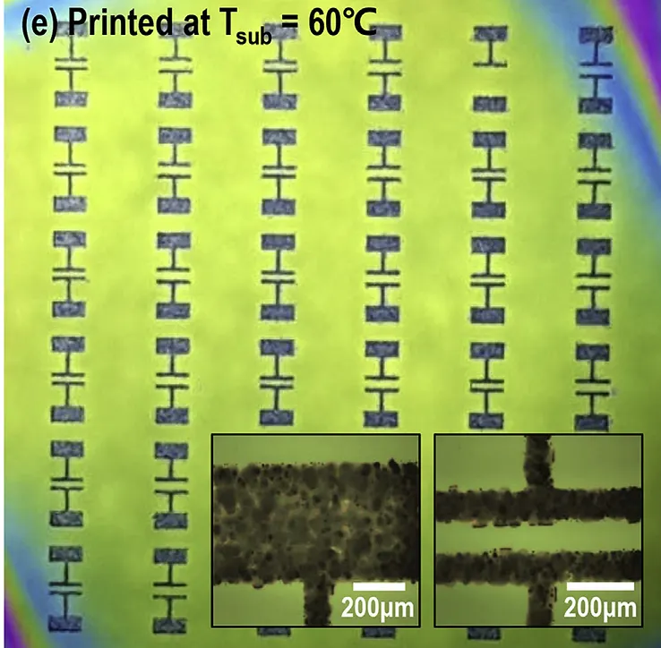
2. Pen Printing
The molecular orientation and crystallinity of polymers are one of the most important factors in the performance of organic electronic devices. Depending on the crystallinity, the mobility of the OTFT may vary several orders of magnitude.
Polymer arrangements that are advantageous for performance enhancement include edge on structure, large grain size, and spherulite formation in low molecular weight materials.
We are studying to produce high performance electronic devices through favorable molecular alignment and high crystalline arrangement of polymers.
Sensors
1. Strain Sensors
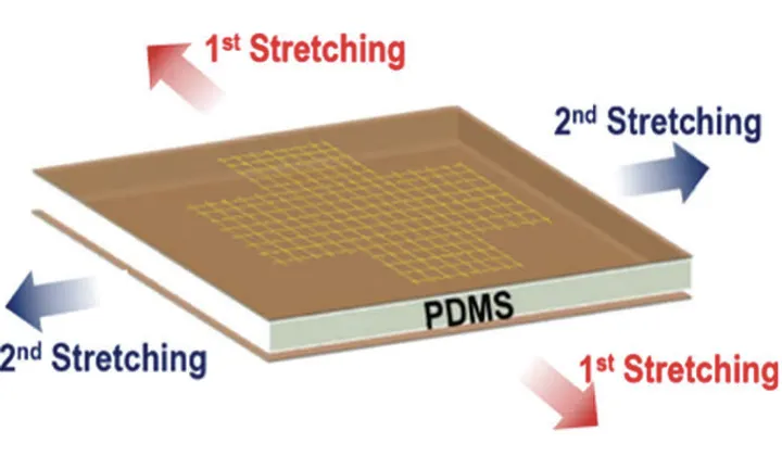
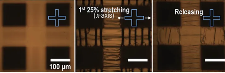
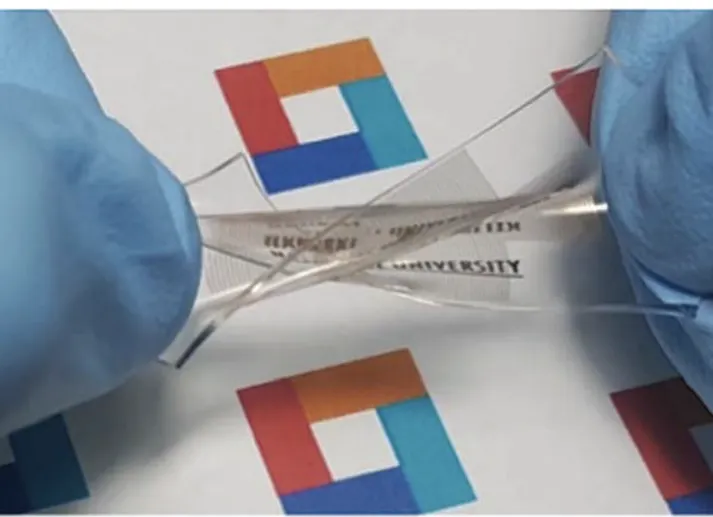
Flexible strain sensors are a key component of electronic skin (e-skin), a technology that is currently receiving considerable research attention with a view to future applications ranging from human healthcare monitoring to robotic skins and environmental risk detection. Here, we developed a highly sensitive, simple, and low-cost piezoresistive strain sensor, which acted as a flexible reactive resistor with a cracked microtectonic architecture that could be fabricated over a large area. In particular, our strain sensor recognizes the direction of tensile stimulation through its rational crisscross electrode design, allowing it to overcome some of the shortcomings of traditional flexible strain sensors. Under a given stress, the strain sensor developed here showed a variation in the relative resistance (ΔR/R0) of up to 24-fold depending on the direction of the applied stress. For example, application of a 1% strain changed ΔR/R0 by 0.11 when the strain was applied parallel to the direction of current flow, but by only 0.012 when the strain was applied perpendicular to that direction. Similarly, a 5% strain changed ΔR/R0 by 0.85 and 0.062, and a 20% strain changed ΔR/R0 by 2.37 and 0.098, depending on whether the strain was applied parallel or perpendicular to the current flow, respectively. In addition, ΔR/R0 varied approximately linearly as a function of the strain over the operational range. The results thus show that the proposed sensor is sensitive to the direction in which an external stress is applied. Finally, we demonstrated that our sensor could be used to detect the bending of a human finger.
2. Pressure Sensors
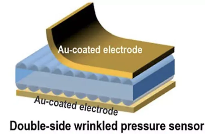
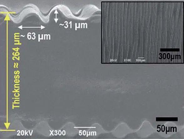
Flexible pressure sensors are a key component of electronic skin (e-skin) for use in future applications ranging from human healthcare monitoring to robotic skins and environmental risk detection. Here, we demonstrated the development of a highly sensitive, simple, and low-cost capacitive pressure sensor, which acted as a flexible capacitive dielectric, based on a microstructured elastomeric template that could be fabricated over a large area. To achieve this goal, the dielectric template was prepared simply by stretching and releasing a flexible Ecoflex film to produce wrinkled surface microstructures with a feature size on the order of tens of micrometers. The effects of the wrinkled surface microstructure on the sensing performance were systematically investigated by comparing the nonwrinkled film, one-side wrinkled film, and double-side wrinkled film. The response and release times of the double-side wrinkled pressure sensor were improved by 42% and 25% in comparison with the values obtained from the unwrinkled case, respectively. These results showed that the introduction of wrinkled surface microstructures to the elastomeric template efficiently enhanced the pressure sensor performance. We also demonstrated that our sensor could be used to detect a variety of changes in the surroundings, such as variations in the angle of a stimulus, object loading/unloading, or an exhaled breath.
본 연구진은 유연한 정전용량식 압력 센서 역할을 하는 대면적 미세구조 엘라스토머 템플릿을 제작하기 위한 간단하고 저렴한 공정을 설계하였다. Ecoflex 유전체 박막을 양쪽으로 늘린 후 UVO 처리를 통해 규산염 층을 형성시켰고, Ecoflex 필름의 변형이 완화되면서 수십 마이크로미터 정도의 주름진 미세구조가 형성되었다(그림 7a). 여기에 Au가 코팅된 실리콘 웨이퍼와 PDMS를 각각 Ecoflex template 상단과 하단에 배치하여 전극을 형성시켜 주름진 구조를 갖는 유연 압력센서를 제작하였다. 주름이 없는 필름, 단면 주름 필름, 양면 주름 필름을 비교하여 주름진 표면 미세구조가 감지 성능에 미치는 영향을 체계적으로 조사하였다. 양면 주름형 압력센서의 응답속도와 해제시간은 주름이 없는 경우에 비해 각각 42%, 25% 개선되었다(그림 7b). 이러한 결과는 엘라스토머 템플릿에 주름진 표면 미세구조의 도입이 압력 센서 성능을 효율적으로 향상시킴을 보여주었다. 개발된 압력센서는 높은 감도, 빠른 응답성, 우수한 내구성 및 성능 반복성을 바탕으로 책을 펼치거나 물체의 유무, 그리고 내쉬는 호흡과 같은 주변의 다양한 변화를 감지하는 데 사용될 수 있음을 확인하였다(그림 7c-e).
3. Chemical Sensors
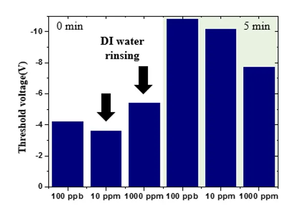
A person's sweat contains various ingredients, and the composition of sweat changes according to a person's health condition. Lactic acid, one of the components of sweat, is a chemical component that is an indicator of fatigue. Lactic acid is produced in cells during anaerobic exercise, which is accumulated in the muscles when fatigued, and causes fatigue in the body. In addition, lactic acid can be a good indicator of pathological disorders. Lack of oxygen in the blood, especially when the sweat gland cells produce lactic acid, the concentration of lactic acid in the sweat increases. This means that a disease that causes hypoxia can be diagnosed by detecting the concentration of lactic acid. Other studies have shown that lactic acid is a good indicator of reduced oxygen delivery in tissues from patients with peripheral arterial occlusive disease. Therefore, sensors that detect lactic acid may be required not only for personal health care, but also for specialized medical applications.
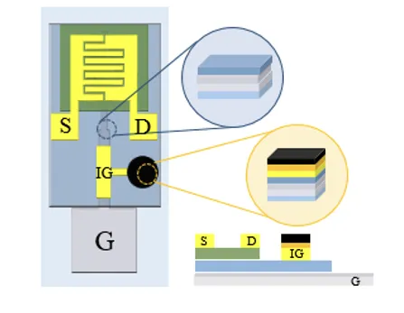
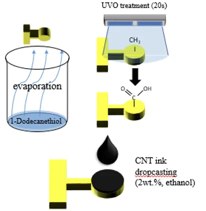
In the present study, we use transistors with a special structure called an interference gate. The interference gate is an electrode located on the dielectric. The sensing principle of this particular device acts as the sensing area of transistor-based sensors and is related to the threshold voltage shift by affecting the transfer characteristics of the transistor depending on the charge applied to the surface. This structure has the advantage of requiring a small amount of sample for detection without requiring a separate reference electrode. Carbon nanotube (CNT) was used as a sensing material in the interference gate sensing area. CNTs have functional groups that can chemically react with other materials such as carboxyl groups. Lactate oxidase (LOD) and peroxidase from horseradish were chemically combined with CNT-COOH to detect lactic acid. LOD oxidizes lactic acid to produce hydrogen peroxide (H2O2), and Peroxidase from horseradish (HRP) causes oxidation-reduction reaction while decomposing H2O2 to enable sensor detection.
Polymer Composites
1. Polymer-based heat dissipation technology
#Thermal-conductive Paste
This refers to enhancing a heat-dissipation capability for securing surface treatment technology to optimize mixing and dispersion between heat dissipation filler and organic binder. It is about finding the best method to combine a material that helps in spreading out heat (heat dissipation filler) evenly with an organic substance that binds or holds everything together (organic binder), ensuring they mix well for effective heat management.
2. Polymer-based EMI technology
# Urethane-Acryl #Electromagnetic Waves #Shielding #Conduction #Adhesive
As the trend of slimming, miniaturizing, and lightening display devices such as smartphones continues, efforts are being made to reduce the thickness, weight, and cost by decreasing the number of films in display panels. However, slimming has led to the high integration of Flexible Printed Circuits (FPC) laminated within the Flexible Copper Clad Laminates (FCCL) in the devices. Additionally, with the transition to higher generations of mobile communication, the increase in communication frequencies has resulted in Electro-Magnetic Interference (EMI) issues, posing challenges to device improvement. The electromagnetic waves emitted or conducted from the front of the device's display have caused malfunctions in other devices and degradation of signal quality. As regulations on EMI become stricter, the demand for electromagnetic shielding materials is increasing. The World Health Organization (WHO) has classified cell phone electromagnetic waves as 'Group 2B,' which is possibly carcinogenic to humans, raising awareness of electromagnetic radiation. The high-conductivity adhesive for electromagnetic shielding developed by our research team will be crucial in addressing EMI and achieving Electro Magnetic Compatibility (EMC) by reducing electromagnetic radiation emissions to a certain level without the need for a separate electromagnetic shielding film when applied within the display.